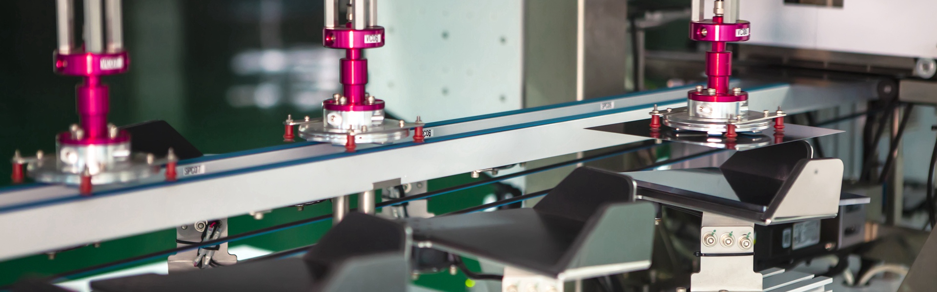
The silicon ingots are cut by mortar or diamond wire to form small silicon ingots with a fixed wafer size after cooling. The small square ingot is fixed on the feed table, and the feed table cuts the silicon ingot into silicon wafers with high-speed moving diamond wire at a certain downward pressure speed.
The company is committed to pursuing products that meet the needs of the current and future photovoltaic market. Successfully developed and launched new high-efficiency mono/poly crystalline silicon wafers which adopted unique ingot casting technology, laid the company's leading position of industry technology.
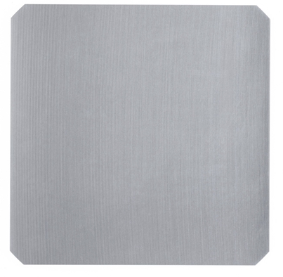
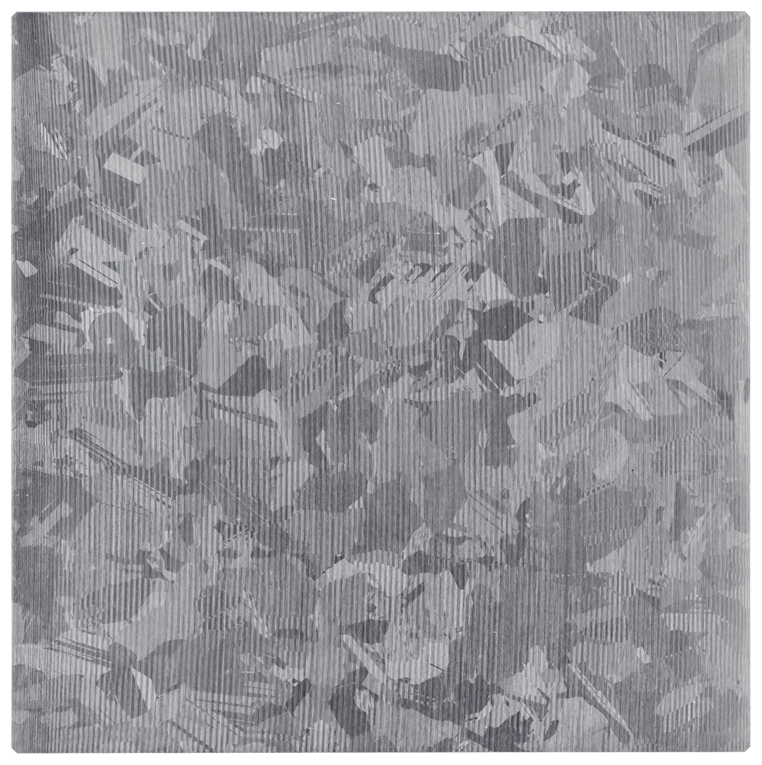
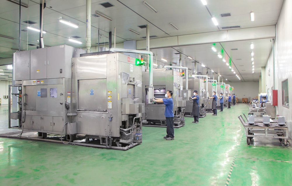
With advanced production equipment and technical strength, the company is constantly to research & develop high efficient products, and applications. A series of high-efficiency poly silicon wafers with independent intellectual property rights, leading poly silicon wafers into high efficiency era. High-efficiency poly crystalline silicon wafers have higher conversion efficiency and the efficiency is more concentrated. The use of diamond wire cutting silicon wafer technology, which is the best in recently world, improves the slicing efficiency. The company's annual supply of multi-silicon wafers is 72 million, with an annual output value of 144 million yuan. The annual supply of mono crystalline silicon is 400 million pieces, and the annual output value reaches 2 billion yuan.
|
|